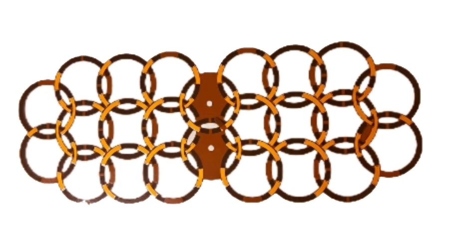
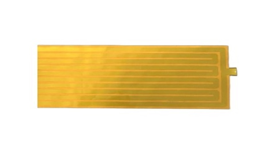
Flexible Printed Circuit Board (Flex PCB) is a special type of circuit board that can be bent into the desired application shape. Compared to ordinary rigid circuit boards, this type of circuit board places conductive paths and electrical components on a flexible substrate. Flexible PCB design has many advantages when building modern compact electronic devices (like phones, cameras, hearing aids, etc.). So if you are a technician involved in such projects, here is a detailed analysis of the design methods and types of the flexible printed circuit board Flex PCB.
While both rigid and flexible PCBs aim to connect electronic components in compact circuit designs, they are different.
The primary distinction lies in the substrate material. Flexible PCBs have a flexible substrate usually composed of polyimide film, whereas rigid types have a fiberglass substrate.
Due to flexing, manufacturers also use flexible rolled annealed copper instead of rigid electrodeposited copper to create the conductive layer.
In producing these components, flexible PCBs use a covering process to protect exposed circuits, whereas rigid types use solder masks. The former is also more expensive, but overall product costs may be cheaper as you can reduce the size of the devices you plan to manufacture.
It depends on the application. Flexible PCBs are ideal for compact electronic devices and appliances like phones, hearing aids, and wearables. However, rigid boards are better suited for devices with larger spaces, such as computers and televisions.
You can combine both to form a rigid-flex board, with half the design in the rigid board and the rest in flexible circuitry.
Basic rigid PCBs require only Gerber file layers during the design phase. However, the rigid flex pcb needs 3D design software to create the board in 3D space before manufacturing.
They have more dimensions, necessitating precise definition of the transition points from flexible to rigid, making 3D design essential.
The base film on the flexible side is polyimide, with a copper foil and overlay retention film layer on top. However, rigid PCBs use FR4 as the substrate.
The first step is to apply accessible adhesive to the copper layers during the assembly process. After that, you can proceed with either the copper plating method or covering process for the next stage.
Upon completion, use precise laser drilling methods to create holes in the flexible substrate.
Then, fill these holes with copper using the through-hole plating process (electroplated copper synthesis).
The next steps include applying photoresist etching on the flexible surface and then etching the copper film.
After that, an overlay (usually polyimide) is applied to the top and bottom layers of the flexible substrate.
Following this, the board undergoes a blanking process, cutting the substrate into the required dimensions. The most common blanking methods are hydraulic die or kick and die set.
Finally, the cut flexible blanks are layered between the rigid layers. The final piece can then be tested to ensure it functions correctly.
Space and weight savings.
Increased stability and reliability
No need for connectors and wiring harnesses, minimizing wiring errors
Can be stacked in various configurations
High tensile strength and high resistance to radiation, chemicals, and extreme temperatures
Durable (suitable for harsh environments)
Easy to install
Provides strong signal quality
Improved impedance control

Higher cost compared to rigid PCBs in specific applications
Requires complex assembly process
Difficult to repair or rework
Needs proper storage conditions
Easily damaged if mishandled
As the simplest type, single-sided flexible circuits have a single conductive layer on one side of the dielectric layer (polyimide or polymer film).
Double-Sided Flex PCBs have a conductive copper layer on each side of the dielectric material. Metallized vias connect the two copper edges.
This type contains multiple copper layers separated and encapsulated by dielectric layers. Through-holes that connect each of the metalized layers.
As mentioned earlier, Rigid-Flex PCBs are multilayer circuits that combine rigid and flexible boards to form a hybrid design with high circuit density.
High Density Interconnect (HDI) circuits are efficient and reliable circuit boards with multiple electronic components. They offer better electrical performance in a smaller package size due to the use of thin, non-conductive substrate materials.
This is a special type of single-sided PCB where the conductive tracks can be accessed from either side of the board.
Two things make this possible. First, a metal layer has a pre-punched dielectric film applied to it. Second, the conductor layer is etched below the access points (openings) on the flexible film (dielectric).
Flexible PCBs consist of multiple layers, but the number varies depending on the type. These schematics and stackups can help you build a design process in.
Single-Sided FPCBs have a simple stack consisting of a flexible base layer (usually polyimide) followed by an adhesive layer and then copper. A protective layer (overlay) consisting of adhesive and polyimide covers the metal. However, the conductive parts must not be exposed.
This PCB utilizes a flexible laminate material as a substrate to separate the conductive layers. Each metal layer has an overlay to protect the circuitry and copper-plated vias to connect the two sides.
Multi-Layer Flex combines single-sided and double-sided flexible circuit designs. Inside, the middle section has double-sided flexible circuitry, while the surface has a single-sided conductive design covered with a protective film.
Like the single-layer circuit, this circuit has five layers, but with one difference. The polyamide outer layer on the base has a laser opening to access the copper circuit.
The four main layers in a flex board can have the following materials.
The metal used in this layer is usually copper because of its excellent electrical properties and low cost. Heat dissipation is also a key factor to consider, which copper can quickly do. Other suitable conductor materials include stainless steel, beryllium copper and white copper.
An adhesive layer containing acrylic or epoxy resins sits between the copper and the insulating film (polyimide). Acrylic adhesive materials offer better heat resistance but have poor electrical properties and lower bond strength.
On the other hand, epoxy is not the best for heat resistance, but it offers better electrical properties and adhesion.
Source: Wikimedia Commons
Insulators, also known as substrates or dielectrics, are flexible materials that give this board its bending properties. Polyimide is the most commonly used material, but some boards are available in polyester, polyetherimide, various copolymers, or fluoropolymers.
High speed digital/RF/microwave connectors
Industrial sensors
Instrumentation consumables
Medical Devices - Wearables
Automotive
Satellite
Avionics
Consumer Electronics
We specialize in multilayer flexible and rigid-flexible manufacturing and offer SMT component assembly for these boards.
We assure you of quality, reliability and durability, which means you can use our products in high-temperature, high-density applications without worry.
In addition, our prices are reasonable and our lead times for flexible and rigid-flex PCBs are 2-13 business days and 6-16 business days, respectively. Build time varies depending on design, quantity, etc. Feel free to contact us by selecting the appropriate contact method for your inquiry.
In summary, Flexible PCBs from bolion are ideal for building compact packages and devices due to their bending properties. If your project requires this type of circuitry, please contact us for more detailed information about flexible PCBs and to get the best quote for your design.
 Advantages and Applications of Polyimide Film Heater
16 Apr 2025
Polyimide film heater is a high-performance electric heating element made by using polyimide film as the outer insulation layer, metal foil or metal wire as the inner conductive heating element, and b...
 Call us on:
  Email Us:
  No.198 Houxiang Road, Haicang District, Xiamen, China